Article
CHIP DESIGN: ASIC Design in a Reliable Supply Chain
Bruco IC's full turnkey ASIC development process in the Netherlands, from feasibility assessment and definition to design and supply chain.
Over the past decades, driven by lower costs and higher volumes, there has been a strong tendency to shift the semiconductor supply chain to the Far East. Gradually, development and R&D followed suit. Since 2019, the geopolitical winds have shifted dramatically, and the importance of an independent semiconductor supply chain in the West is being recognized. How does a company like Bruco IC develop ASICs in the Netherlands?
At Bruco IC, we deliver IC design services to a wide range of customers. These services can be divided into three types:
Our typical ASIC customers are OEMs without their own IC design team, who develop electronic applications using discrete electronic components. These OEMs may decide to go into production with a PCB, but when volumes increase or when very small dimensions are required, the need for miniaturization arises, leading to the demand for an ASIC. A typical ASIC development project can take 2-4 years, and with Non-Recurring Engineering (NRE) costs running into several million euros, it is not a decision taken lightly.
The ASIC development process starts with a high-level feasibility assessment. One of our system architects delves into the concept, performs some high-level modeling, and determines which technology can be used, for example, plain CMOS, BCD, or SiGe. The outcome is that we can, in principle, design the ASIC, and we have a clear idea of the process technology node to be used. This feasibility assessment typically takes 2–3 months.Once the customer accepts the outcome of the high-level feasibility assessment, an official feasibility study can be initiated.
Milestone: ATS (Acceptance Type Study)
This phase includes the high-level IC requirements specification, IP block specification, IP block design, and the definition of the IP block area, supported by a risk assessment. To meet the customer's requirement for an early cost estimate, we must assess the initial IC area, select the process, foundry, packaging partner, and assembly house, and create a high-level project schedule. Depending on the complexity of the ASIC, this phase lasts 3–6 months and concludes with a report and the achievement of the ATS milestone.
Production Partners (Examples):
For an RF project requiring a 130nm SiGe process node, options include Globalfoundries and IHP in Germany, and the Israeli Tower Semiconductor (part of Intel). For a 9x9-mm QFN64 package, we can turn to Amkor or ASE with assembly in the Far East. Due to the generally lower volumes of ASICs, Sencio's functional packaging center in Nijmegen is a good alternative to the larger companies.
ATS is followed by the definition phase, which results in the ATD milestone.
Milestone: ATD (Acceptance Type Development)
During this phase, further details are added to the IC requirements and IP block specifications, and a more accurate IC area estimation is provided, along with a more precise cost estimate. At this point, the customer has all the information to make the go/no-go decision for the actual design. In parallel, Design for Test (DfT) is added to improve testability. Salland Engineering in Zwolle is our preferred partner for this. The definition phase can take between 3–4 months.
Now it is time for the actual design trajectory, involving a team of IC designers, verification and validation engineers, an IC system architect, and a project manager, supplemented by a supply chain coordinator. A weekly PMO (Project Manager Office) meeting ensures progress.
First Design Part and Evaluation
Second Design Part and Evaluation
Typically, the validation results lead to design improvements. These are implemented in the second part of the design phase, which is shorter than the first.The subsequent AFM2 milestone involves the final ordering of the mask set. A second silicon verification leads to the SiV2 milestone.
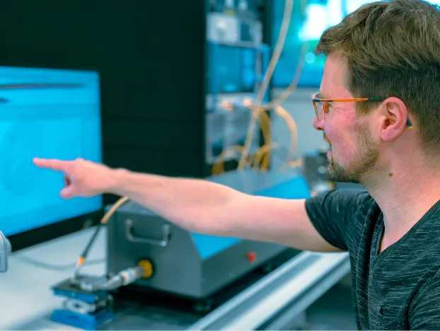
In parallel with validation, the characteristics of the silicon are measured using Automatic Test Equipment (ATE). For qualification, ATE testing is essential for comparing the measurement results before and after reliability testing, and for performing initial electrical failure analyses. Salland Engineering has been our partner here for over ten years.
Milestone: RFS (Release for Supply)
Once the silicon is validated on the ATE bench, we are halfway through the ASIC development journey. Before we can release the product, it must be qualified and achieve the RFS milestone.
A successful ASIC business depends on a reliable, predictable, and trustworthy supply chain. Managing an unstable supply chain is a nightmare, and the last few years, in particular, have demonstrated challenges in capacity, pricing, and lead time.At Bruco IC, we have partners all over the world. Due to all the required interaction, we work as much as possible with flexible local suppliers—in the same time zone, preferably close by.Within the Netherlands and Europe, we have many semiconductor companies, ranging from design houses to fabless chip outfits, IDMs, and OEMs. Wafer foundry services are a global business. Although the US and EU Chip Acts may change this, our strength does not lie, nor should it, in the mass production of single-digit nanometer process nodes, but rather in innovation and combining different types of technologies into one solution. An illustrative example is the new Chip Tech Twente initiative by Kennispark Twente, the University of Twente, and companies in Twente, aimed at developing heterogeneous systems based on photonics, semiconductors, and assembly. The key is open and transparent collaboration within a large partner network. As such, this will likely also boost our supply chain.
Source: Bits & Chips by Nieke Roos
Explore the latest developments in RF IC, analog/mixed-signal design from Bruco Integrated Circuits.
.png)