Case
SiGe BiCMOS LNA and Switch Integration for Mobile Front-Ends
Overcoming process limitations to integrate RF switches with Low Noise Amplifiers in high-volume smartphone applications.
Integrating RF switches directly with a Low Noise Amplifier (LNA) presents a distinct contradiction in semiconductor physics, particularly within a SiGe BiCMOS process. While SiGe BiCMOS offers excellent performance for the amplifier core, it is historically challenging for implementing low-loss, high-linearity switches compared to SOI or CMOS processes. The engineering challenge was to design a "perfect switch" within these process constraints while simultaneously driving down the Noise Figure (NF), minimizing power consumption, and eliminating external matching components to reduce the customer's Bill of Materials (BOM).
The primary technical hurdle involved the switch topology. In standard SiGe BiCMOS, realizing a switch with low insertion loss and high isolation is difficult without compromising the overall system Noise Figure. We had to balance the trade-off between the switch's linearity requirements and the LNA's current consumption.
To reduce the BOM, the design required the removal of external matching components. This forced the integration of matching networks on-die, which typically introduces loss and degrades noise performance. We compensated for this by optimizing the LNA core design to maintain the required gain and NF budget, ensuring the integrated chain met the strict sensitivity requirements of modern handset standards.
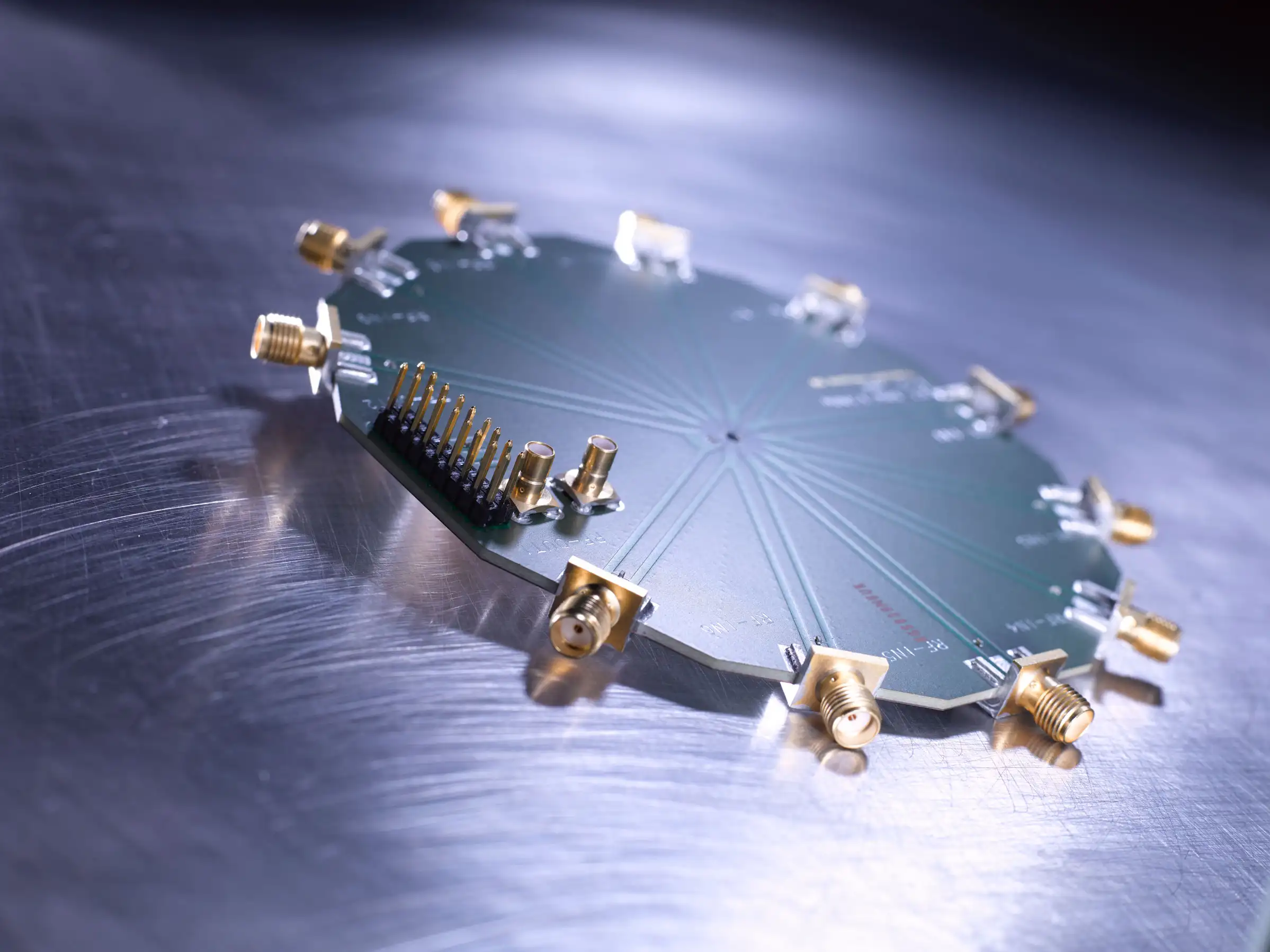
Given the high-volume nature of the target application, reliance on simulation alone was insufficient. We designed a custom multi-input/output LNA evaluation board to characterize the physical silicon across all operating bands.
A critical step in the release process was the correlation of test data. We aligned our internal measurement setup directly with the customer's production test equipment. By correlating our lab results with their specific hardware environment, we eliminated measurement discrepancies before the design entered mass production, preventing yield fallout at the assembly stage.
The silicon met all performance parameters regarding Noise Figure and power efficiency. The reduction in external components simplified the board layout for the end customer. Consequently, this design secured design-ins with several major smartphone manufacturers, validating the approach of integrating switching functions in SiGe BiCMOS when optimized correctly.

Explore the latest developments in RF IC, analog/mixed-signal design from Bruco Integrated Circuits.

.png)